Modules 1 & 2 - NMOS Review
Section 4.2: NMOS Equations
A summary of the needed NMOS equations is as follows:
For all regions:
For the Cutoff Region, when
For the Triode Region, when
For the Saturation Region, when
The Threshold Voltage
Where
There are some other parameters that we use to convert an NMOS to various formats, for instance, the transconductance
SS
Further, the on-resistance is the resistance in the triode region near the origin, given by:
Sections 6.1-6.3: Inverter Characteristics - Digital Paradigm
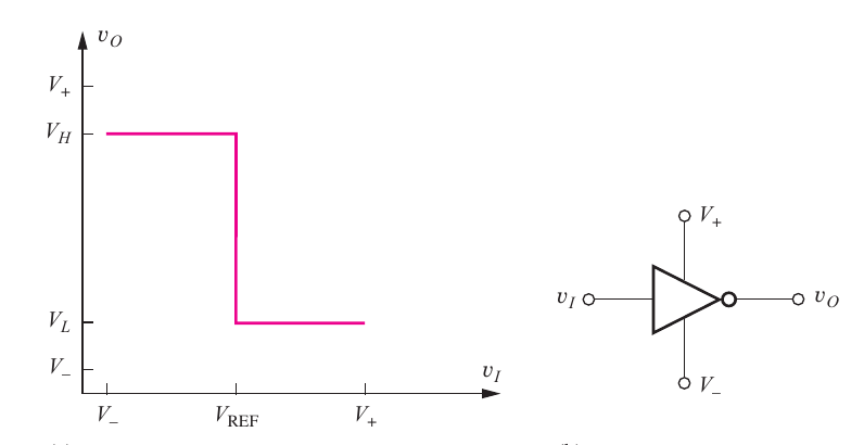
6.1: Ideal Logic Gates
The logic symbol and voltage transfer characteristic (VTC) for an ideal inverter is given in the figure below:
- Under
is a logic low, ie: 0. So for this inverter, is a high logic level at the gate output - Over
we have is low logic level. are the power supply voltages to the gate provided. now and .
6.2: Logic Level Def's and Noise Margins
Really the inverter circuit is a voltage controlled switch:
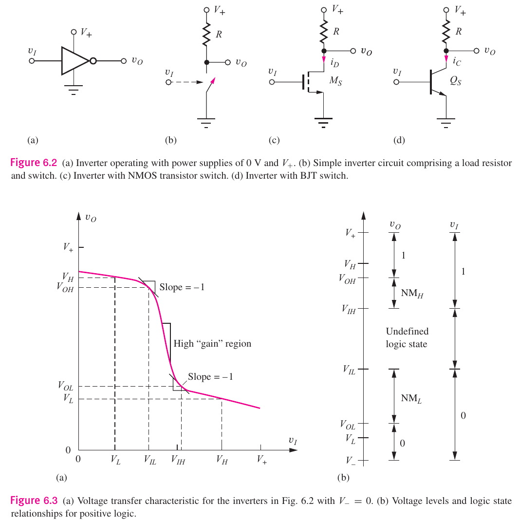
- We either use a MOS transistor
or a bipolar transistor . dictates the highest value when the transistor in question is off (no current flow) often is not 0! We'll see this in later chapters.
The transfer curve in 6.3(a) shows how the transition from
When
The nominal voltage corresponding to low-logic state at the output when . Generally, . The nominal voltage corresponding to high-logic state at the output when . Generally . The max input voltage recognized as a low logic signal The min input voltage recognized as a high logic signal The output voltage corresponding to an input voltage of The output voltage corresponding to an input voltage of
For our purposes
6.2.2 Noise Margins
- Noise Margin in the high state
and same for the low state are the margins allowed in the case that noise is introduced in the input to produce erroneous output
There may be resistance, capacitance, or inductance introduced into a PCB, thus we may have a lot of error over large amounts of gates. Using the definitions of the -1 slope points described above, we have the following:
If a TTL gate has
6.2.3 Logic Gate Design Goals
Goals for logic gates:
- Minimize the width of the undefined input voltage range (ie: high noise margins)
- Input shouldn't be affected by Output
- Similar values of
should be used among all gates - There should be allowed to have many different inputs to control one output, and many output to control an input of another gate
- It should consume little power
6.3 Dynamic Response of Logic Gates
The clock speed of a processor is bottle necked by the propagation delay, rise time, ..., which are all things we now have control of.
6.3.1 Rise and Fall Time
rise time 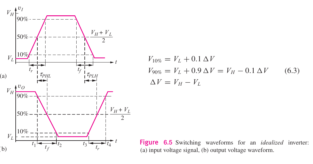
Here:
6.3.2 Propagation Delay
Propagation Delay is the difference in time between the input and output signals reaching their 50% mark. The 50% point (in volts) is defined as:
The propagation delay on the high-to-low output transition is
Look at [[Pasted image 20240115202148.png]]. If
Proof
We know that:
☐
6.3.3 Power-Delay Product
There's a power cost to switching a wire from 0 to 1 or vice versa, and for a whole gate there's an additive total cost. In low power regions, gate delay is dominated by inter gate wiring capacitance. But if we increase the power and device size, then we get limited by the speed of the electronic switching itself.
For our low-power purposes, we have it that the propagation delay decreases in direct proportion to the increase in power, so then the power-delay product (PDP) is defined as:
where