The worst case occurs by looking at the longest PMOS and NMOS network path, and dividing the number of transistors over the overall range of .
For PMOS:
and for NMOS:
Thus for :
and:
Thus .
Using .
73
a
The device implements .
b
c
When all NMOS are on, then we get an effective 3 transistors in series (worst-case) and two in parallel, giving:
d
For the PMOS we get 3 transistors now in parallel, and 2 in series, giving:
Domino Logic
97
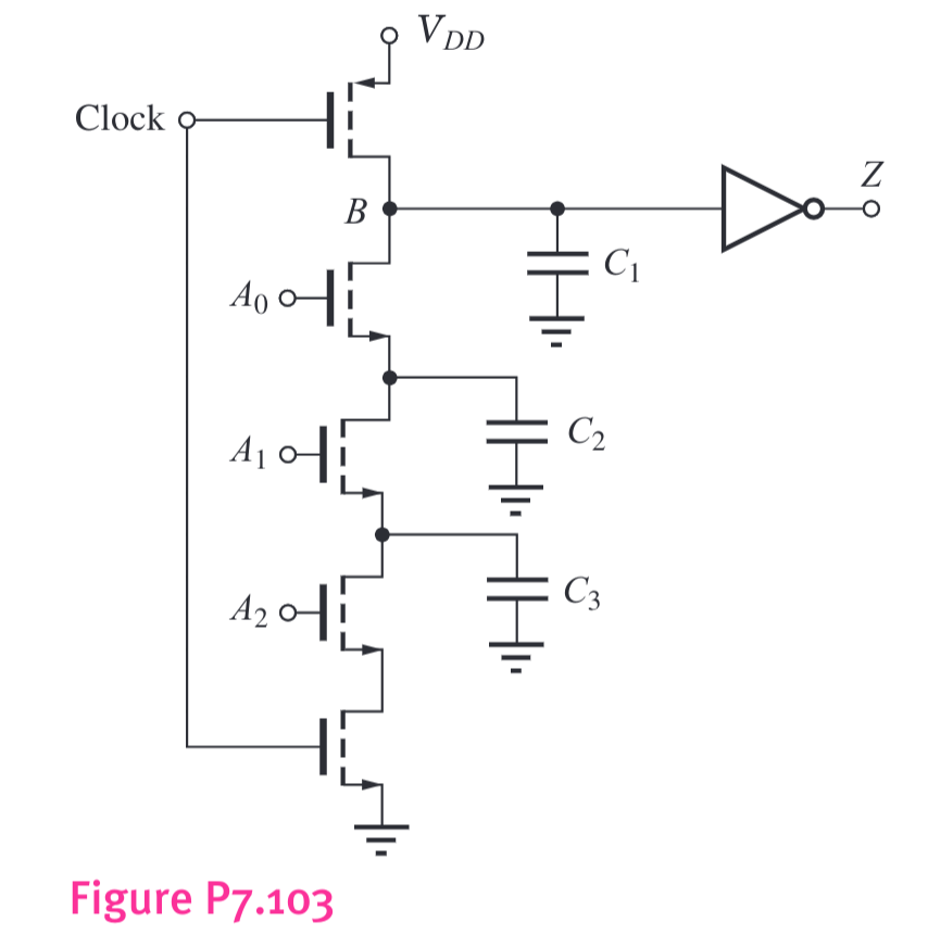
103
We're given:
a
Assuming all from the circuit, then going into the evaluate phase (clock when high), while we have assumed that 's are still uncharged (as we just entered the phase). If at this moment, then the voltage at node has charge sharing between (as the related MOS becomes a short, connecting the tops of and ).
Thus we can use:
Thus for :
Where we know that prior to the switch must be as it's uncharged, and similar for . As such:
Hence is two- thirds of the .
b
Now when is changed then we get a similar scenario, where since then our total capacitance is now 4 times as large. Hence we get charge sharing over all capacitors. Here and as before so then we get:
so then the voltage gets halved.
c
In the worst case we have our case from (b) (notice if all are on we get that the capacitor just discharges), hence we need to have be such that: