HW 1 - NMOSReview + Inverter Characteristics
Chapter 4.2
4.9
Known (for NMOS):
V G S = 0 , 1 , 2 , 3 V D S = 0.25 W = 5 μ m , L = 0.5 μ m , V t n = 0.8 V , K n ′ = 200 μ A V 2 We can create a table of each state for each value of V G S
V G S ≥ V t n When we are NOT in cutoff (in this case V G S ≥ V t n
V D S ∘ V G S − V t n = V O V First, we can try to calculate K n
K n = K n ′ ⋅ W L = 200 μ A V 2 ⋅ 5 μ m 0.5 μ m = 2 m A V 2 We make the table using our value for K n
Value of V G S
Value of V O V
Condition on V G S
Condition on V D S
Mode of Operation
Calculation of I D S
0
− 0.8 V V G S < V t n Don't Care
Cutoff
I D S = 0
1
0.2 V V G S ≥ V t n 0.25 = V D S > V O V Saturated
I D S = k n 2 ( V G S − V t n ) 2 = 2 m A V 2 2 ( 1 V − 0.8 V ) 2 = 0.04 m A
2
1.2 V V G S ≥ V t n 0.25 = V D S < V O V Triode
I D S = k n ( ( V G S − V t n ) V D S − 1 2 V D S 2 ) I D S = 2 m A V 2 ( ( 1.2 V ) ( 0.25 V ) − 1 2 ( 0.25 V ) 2 ) I D S = 0.5375 m A
3
2.2 V V G S ≥ V t n 0.25 = V D S < V O V Triode
Same as above, we get:I D S = 2 m A V 2 ( ( 2.2 V ) ( 0.25 V ) − 1 2 ( 0.25 V ) 2 ) I D S = 1.0375 m A
4.15
For this problem, the NMOS has a W / L = 100 V G S = 5 V V t n = 0.65 V K n ′ = 100 μ A V 2
a
The on-resistance is given by the equation:
R o n = 1 K n ′ W L ( V G S − V t n ) = 1 K n ( V G S − V t n ) Thus, we can plug in our values:
R o n = 1 100 μ A V 2 ⋅ 100 1 ( 5 V − 0.65 V ) ≈ 23 Ω b
If instead V G S = 2.5 V V t n = 0.5 V
R o n = 1 100 μ A V 2 ⋅ 100 1 ( 2.5 V − 0.5 V ) = 50 Ω 4.21
Given:
V G S = 0 , 1 , 2 , 3 V , V D S = 4 V , W = 10 μ m , L = 1 μ m , V t n = 1.5 V , K n ′ = 200 μ A V 2 First, we can try to calculate K n
K n = K n ′ ⋅ W L = 200 μ A V 2 ⋅ 10 μ m 1 μ m = 2 m A V 2 We do something similar to HW 1 - NMOSReview#4.9 :
Value of V G S
Value of V O V
Condition on V G S
Condition on V D S
Mode of Operation
Calculation of I D S
0
− 1.5 V V G S < V t n Don't Care
Cutoff
I D S = 0 A
1
− 0.5 V V G S < V t n Don't Care
Cutoff
I D S = 0 A
2
0.5 V V G S ≥ V t n 4 = V D S > V O V Saturation
I D S = k n 2 ( V G S − V t n ) 2 I D S = 2 m A V 2 2 ( 2 V − 1.5 V ) 2 I D S = 0.25 m A
3
1.5 V V G S ≥ V t n 4 = V D S > V O V Saturation
Same as above, we get:I D S = 2 m A V 2 2 ( 3 V − 1.5 V ) 2 = 2.25 m A
4.22
Given:
K n ′ = 200 μ A V 2 , W / L = 10 , V t n = 0.75 V Notice then, for future calculations, that:
K n = K n ′ ⋅ W / L = 2 m A V 2 a
We have:
V G S = 2 V , V D S = 2.5 V We have then V G S ≥ V t n
V O V = 1.25 V , 2.5 V = V D S > V O V = 1.25 V So we are in the saturation region, so then:
I D = K n 2 ( V G S − V t n ) 2 = 2 m A V 2 2 ( 2 V − 0.75 V ) 2 = 1.5625 m A b
We have:
V G S = 2 V , V D S = 0.2 V We have then V G S ≥ V t n
V O V = 1.25 V , V D S < V O V So we are in the triode region:
I D = K n [ ( V G S − V t n ) V D S − 1 2 V D S 2 ] = 2 m A V 2 [ ( 1.25 V ) ( 0.2 V ) − 1 2 ( 0.2 V ) 2 ] = 0.46 m A c
We have:
V G S = 0 V , V D S = 4 V We have that V G S < V t n cutoff . Thus, I D = 0 A
d
We replace our K n ′ 300 μ A V 2
K n = K n ′ ⋅ W / L = 3 m A V 2 The findings are in the same regions as before, just with slightly different values:
Problem Part Region of Operation
I D
a
Saturation
I D = 3 m A V 2 2 ( 2.0 V − 0.75 V ) 2 I D = 2.344 m A
b
Triode
I D = 3 m A V 2 [ ( 1.25 V ) ( 0.2 V ) − 1 2 ( 0.2 V ) 2 ] I D = 0.69 m A
c
Cuttoff
0 A
4.27
We are given that:
V G S = 2 V , 3.3 V Separately. In general:
V D S = 3.3 V , W = 20 μ m , L = 1 μ m , V t n = 0.7 V , K n ′ = 250 μ A V 2 Thus:
K n = K n ′ ⋅ W / L = 5 m A V 2 We can check for the necessary condition of being in the saturation region if we notice first that:
3.3 V = V D S ≥ V G S − V t n = 1.3 V , 2.7 V Depending on whether we use the first, or second value for V G S
V O V = V G S − V t n = 1.3 V , 2.7 V ≥ 0 V Thus we aren't in cutoff, so therefore we are indeed in the saturation region. Thus, we can use the equation for transconductance:
g m = K n ( V O V ) = 6.5 , 13.5 m A V = 6.5 , 13.5 m S For the corresponding values of V G S
4.30
Given:
K n = 500 μ A V 2 , V t n = 1 V , V G S = 4.0 V , V D S = 5.0 V For both parts, notice first that V O V = V G S − V t n = 3.0 V ≥ 0 V D S ≥ V O V
I D = K n 2 ( V G S − V t n ) 2 ( 1 + λ V D S ) a
We first consider when λ = 0.02 V − 1
I D = 0.5 m A V 2 2 ( 3.0 V ) 2 ( 1 + 0.02 V − 1 ⋅ 5.0 V ) = 2.475 m A b
We now consider when λ = 0 V − 1
I D = K n 2 ( V O V ) 2 = 0.5 m A V 2 2 ( 3.0 V ) 2 = 2.25 m A 4.32
We'll find the drain current in the NMOS transistor configuration given by:
First, we get some values for free from Table 4.6:
W / L = 10 ⇒ K n = K n ′ ⋅ W / L = 100 μ A V 2 ⋅ 10 = 1 m A V 2 V t n = 0.75 V Some work before getting into the problem, notice that, we'll just assume that we are in the saturation mode, so then:
I D = I R , 12 V − V D 100 k Ω = I D = K n 2 ( V G S − V t n ) 2 ( 1 + λ V D S ) a
We first consider λ = 0
You can't use 'macro parameter character #' in math mode \begin{align} \frac{12V - V_{GS}}{100k\Omega} &= \frac{1 \frac{mA}{V^2}}{2}(V_{GS} - 0.75V) { #2 } \\ \Rightarrow 12V - V_{GS} &= 50(V_{GS}^2 - 1.5V_{GS} + 0.5625V) \\ 12V - 28.125V &= 50V_{GS}^2 - 74V_{GS} \\ 0 &= 50V_{GS}^2 - 74V_{GS} + 16.125V\\ \Rightarrow V_{GS} = \frac{74 \pm \sqrt{74^2 - 4\cdot50\cdot16.125}}{2\cdot 50} &= 1.214V, 0.266V\\ \end{align} \begin{align} \frac{12V - V_{GS}}{100k\Omega} &= \frac{1 \frac{mA}{V^2}}{2}(V_{GS} - 0.75V) { #2 } \\ \Rightarrow 12V - V_{GS} &= 50(V_{GS}^2 - 1.5V_{GS} + 0.5625V) \\ 12V - 28.125V &= 50V_{GS}^2 - 74V_{GS} \\ 0 &= 50V_{GS}^2 - 74V_{GS} + 16.125V\\ \Rightarrow V_{GS} = \frac{74 \pm \sqrt{74^2 - 4\cdot50\cdot16.125}}{2\cdot 50} &= 1.214V, 0.266V\\ \end{align} We know that V G S ≥ V t n = 0.75 V V G S = 1.214 V
V G S = 1.214 V ⇒ I D = 0.108 m A b
We do the same thing except when λ = 0.025 V − 1 V D S = V G S
12 V − V G S 100 k Ω = 1 m A V 2 2 ( V G S − 0.75 ) 2 ( 1 + λ V G S ) 12 V − V G S = 0.5 m A V 2 ( V G S 2 − 1.5 V G S + 0.5625 ) ( 1 + 0.025 V G S ) We can intersect the LHS function with the RHS function to see where they intersect on a graphing calculator. This gives:
V G S = 1.15 V ⇒ I D = 108.5 μ A c
If we repeat HW 1 - NMOSReview#a then we get that W / L = 25
K n = K n ⋅ W / L = 100 μ A V 2 ⋅ 25 = 2.5 m A V 2 So then:
12 V − V G S 100 k Ω = 2.5 m A V 2 2 ( V G S − 0.75 V ) 2 ⇒ 12 V − V G S = 250 ( V G S 2 − 1.5 V G S + 0.5625 V ) ⇒ 0 = 250 V G S 2 − 374 V G S + 128.625 V ⇒ V G S = 0.960 V , 0.536 V Again we know V G S ≥ V t n V G S = 0.960 V
I D = 110 μ A 4.34
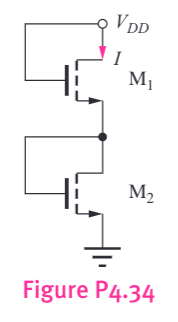
Consider the following:
V G S 1 = V D S 1 V G S 2 = V D S 2 V D D = 10 V = V D S 1 + V D S 2 Saturation , and check that both V G S ≥ V t n V D S > V G S − V t n
I D = K n 2 ( V G S − V t n ) 2 ( 1 + λ V D S ) for various λ
a
Assume that M 1 , M 2 I D I D 1 = I D 2 = I M 1 , M 2 W / L K n K n ′
K n 2 ( V G S 1 − V t n ) 2 ( 1 + λ V G S 1 ) = K n 2 ( V G S 2 − V t n ) 2 ( 1 + λ V G S 2 ) Simplify both sides and substitute λ = 0
( V G S 1 − V t n ) 2 = ( V G S 2 − V t n ) 2 V G S 1 − V t n = V G S 2 − V t n V G S 1 = V G S 2 Thus since V G S 1 + V G S 2 = 10 V V G S 1 = 5 V = V G S 2 > V t n = 0.75 V Saturation . Further, V D S 1 = 5 V > V G S 1 − V t n = 4.25 V K n = W / L ⋅ K n ′ = 10 ⋅ 100 μ A V 2 = 1 m A V 2
I D = 1 m A V 2 2 ( 5 V − 0.75 V ) 2 = 9.03 m A b
We repeat except that W / L = 20 K n = 20 ⋅ 100 μ A V 2 = 2 m A V 2
I D = 2 m A V 2 2 ( 5 V − 0.75 V ) 2 = 18.06 m A c
We repeat, except using λ = 0.04 V − 1
( V G S 1 − V t n ) 2 ( 1 + λ V G S 1 ) = ( V G S 2 − V t n ) 2 ( 1 + λ V G S 2 ) ( V G S 1 2 − 2 V t n V G S 1 + V t n 2 ) ( 1 + λ V G S 1 ) = ( V G S 1 2 − 2 V t n V G S 1 + V t n 2 ) ( 1 + λ V G S 1 ) . . . One needn't check that since the polynomial on the LHS and RHS are the same, we can easily determine that V G S 1 = V G S 2 = 5 V V G S > V t n V D S > V G S − V t n M 1 , M 2
I D = 1 m A V 2 2 ( 5 V − 0.75 V ) 2 ( 1 + 0.04 V − 1 ⋅ 5 V ) = 10.84 m A 4.43
We are given:
V G S = 0 , 1 , 2 , 3 V V D S = 4 V W = 10 μ m L = 1 μ m V S B = 1.5 V And given the Table's data:
V t o = 0.75 V γ = 0.75 V 2 ϕ F = 0.6 V K n ′ = 100 μ A / V 2 We know for an NMOS transistor that:
V t n = V t o + γ ( v S B + 2 ϕ F − 2 ϕ F ) So then we can solve for V t n
V t n = 0.75 V + 0.75 V ( 1.5 V + 0.6 V − 0.6 V ) = 1.256 V We know:
K n = K n ′ ⋅ W / L = 10 ⋅ 100 μ A V 2 = 1 m A V 2 We do something similar to HW 1 - NMOSReview#4.9 :
Value of V G S
Value of V O V
Condition on V G S
Condition on V D S
Mode of Operation
Calculation of I D S
0
− 1.256 V V G S < V t n Don't Care
Cutoff
I D S = 0 A
1
− 0.256 V V G S < V t n Don't Care
Cutoff
I D S = 0 A
2
0.744 V V G S ≥ V t n 4 = V D S > V O V Saturation
I D S = 1 m A V 2 2 ( 2 V − 1.256 V ) 2 = 0.278 m A
3
1.744 V V G S ≥ V t n 4 = V D S > V O V Saturation
I D S = 1 m A V 2 2 ( 3 V − 1.744 V ) 2 = 1.521 m A
Chapter 6.1-3
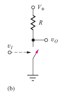
6.3
We are given the following inverter circuit:
We know then that since it's ideal, when V I > V I H V O = V L V O = 0 V O = V +
a
R = 100 k Ω V + = 2.5 V V o = V H = 2.5 V I R = 0 V o = 0.0 V
I R , V o = 0 = 2.5 V − 0 V 100 k Ω = 25 μ A Thus, the power draw for each of when we have:
P V H = I R , V H 2 R = 0 2 ⋅ 100 k Ω = 0 W and:
P V L = I R , V L 2 R = ( 25 μ A ) 2 ⋅ 100 k Ω = 62.5 μ W b
We have the same reasoning as before, so we get:
I R , V o = 0 = 3.3 V − 0 V 100 k Ω = 33 μ A Thus:
P V H = I 2 R = 0 2 ⋅ 100 k Ω = 0 W P V L = ( 33 μ A ) 2 ⋅ 100 k Ω = 108.9 μ W 6.4
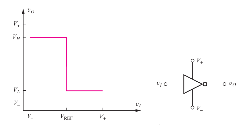
We'll plot the voltage transfer characteristic for an ideal inverter with V + = 2.5 V V − = 0 V V R E F = 0.8 V V H = V + V L = V −
6.5
a
We do the same thing as HW 1 - NMOSReview#6.4 , but with two cascaded inverters:
b
The overall logic expression is Z = f ( A ) = A
6.6
We may want to see our other graph from Figure 6.1 to help us draw this:
A v = ∂ v o ∂ v i
In essence, in the ideal case $A_v$ is just the *dirac delta function* $\delta(v_i) = v_o$.
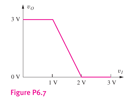
6.7
Given the graph:
V H , V L , V I H , V I L
V H = 3 V , V L = 0 V , V I H = 2 V , V I L = 1 V The A v
6.8
If we had two cascaded inverters following Figure:
Then we'd get the following complete graph...
Essentially here, if the function given is some $f(v)$, then we are considering the cascade as a composition of two of said function $f\circ f$.
6.9
Given that V H = 5 V , V L = 0 V , V R E F = 2.0 V
V I H = V I L = 2.0 V V O H = 5 V , V O L = 0 V Therefore:
N M L = V I L − V I H = 0.0 V N M H = V O H − V O L = 5 V 6.10
We should ideally have V R E F V H V L
V R E F = V H + V L 2 = 1.65 V Note that this works for our noise margins to, specifically the one for our outputs gets maximized:
N M H = V O H − V O L = 3.3 V − 0 V = 3.3 V N M L = V I L − V I H = 0.0 V 6.20
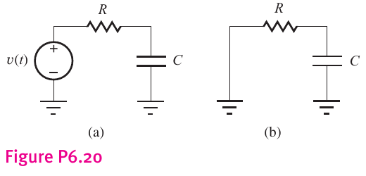
We consider the following circuits:
a
We can just use the equation for a series RLC circuit:
V C ( t ) = V S [ 1 − exp ( − t R C ) ] + V c ( 0 ) exp ( − t R C ) Here we have V S = 1 V V c ( 0 ) = 0 V
V C ( t ) = 1 − exp ( − t R C ) Note that we'll use R C = τ t r V 10 % V 90 % V H = 1 V V L = 0 V
V 10 % = 0.1 V , V 90 % = 0.9 V Thus we need to find the times V c ( t 10 % ) V c ( t 90 % )
V c ( t 10 % ) = 1 − exp ( − t 10 % τ ) = 0.1 ⇒ − ln ( 0.9 ) τ = t 10 % In a similar way we derive that:
⇒ − ln ( 0.1 ) τ = t 90 % Thus, in this case to get the rise-time t r
t r = t 90 % − t 10 % = τ ( ln ( 0.9 ) − ln ( 0.1 ) ) ≈ 2.197 τ Thus, t r ∝ τ
b
In a similar way to HW 1 - NMOSReview + Inverter Characteristics#a , we know that now:
V C ( t ) = exp ( − t τ ) So then, using the same V H , V L
V c ( t 10 % ) = exp ( − t 10 % τ ) = 0.1 V ⇒ − τ ln ( 0.1 ) = t 10 % And likewise:
⇒ − τ ln ( 0.9 ) = t 90 % Thus, to get the fall-time t f
t f = t 10 % − t 90 % = τ ( ln ( 0.9 ) − ln ( 0.1 ) ) ≈ 2.197 τ Thus, t f ∝ τ
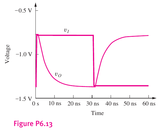
6.22
Consider the graph:
(a) Here V H ≈ − 0.8 V V L ≈ − 1.4 V
(b) The rise and fall times for V I V o t 10 % V 10 % ≈ − 1.34 V t 10 % ≈ 20 n s t 90 % ≈ 2.5 n s
t f ≈ 20 n s − 2.5 n s = 17.5 n s (c) We note that τ P H L ≈ τ P L H V 50 % ≈ − 1.1 V t 50 % ≈ 8 n s
τ P L H = t 50 % − t 90 % = 8 n s − 2.5 n s = 6.5 n s Likewise τ P H L ≈ 6.5 n s
(d) Since τ P H L ≈ τ P L H τ = τ P H L = 6.5 n s